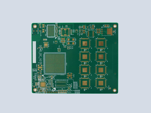
PCB multilayer board refers to the multi-layer circuit board used in electrical products, which uses more single-panel or double-panel wiring boards. A printed circuit board with one double-sided as inner layer, two single-sided as outer layer or two double-sided as inner layer and two single-sided as outer layer, through the positioning system and insulating bonding materials alternately together and the conductive patterns interconnected according to the design requirements, the printed circuit board becomes a four-layer and six-layer printed circuit board, also known asMultilayer circuit board.
With the continuous development of SMT (surface mount technology) and the continuous introduction of a new generation of SMD (surface mount devices), such as QFP, QFN, CSP, BGA (especially MBGA), electronic products become more intelligent and miniaturized, thus promoting the major reform and progress of PCB industrial technology. Since IBM first successfully developed high-density multilayer plates (SLC) in 1991, various groups in various countries have also developed a variety of high-density interconnection (HDI) microporous plates. With the rapid development of these processing technologies, the design of PCB has gradually developed to the direction of multi-layer and high-density wiring. Multilayer PCB has been widely used in the production of electronic products because of its flexible design, stable and reliable electrical performance and superior economic performance.
1. Signal layer (Signal Layers)
Altium Designer can provide up to 32 signal layers, including top layer (Top Layer), bottom layer (Bottom Layer) and middle layer (Mid-Layer). The layers can be connected by through hole (Via), blind hole (Blind Via) and buried hole (Buried Via).
(1), top signal layer (Top Layer)
Also known as the component layer, mainly used to place components, for double-layer plates and multilayer boards can be used to arrange wires or copper cladding.
(2), the underlying signal layer (Bottom Layer)
Also known as welding layer, mainly used for wiring and welding, for double-layer plates and multi-layer plates can be used to place components.
(3) Middle signal layer (Mid-Layers)
There can be up to 30 layers, which are used to arrange signal wires in multilayer boards, excluding power and ground wires.
2. Internal Power layer (Internal Planes)
It is usually referred to as the internal electric layer, which only appears in the multilayer plate. The number of PCB layers generally refers to the sum of the signal layer and the internal electric layer. Like the signal layer, the inner electric layer and the internal electric layer, and the internal electric layer and the signal layer can be connected with each other through through holes, blind holes and buried holes.
3. Screen printing layer (Silkscreen Layers)
A PCB board can have up to two screen printing layers, namely the top screen printing layer (Top Overlay) and the bottom screen printing layer (Bottom Overlay), generally white, mainly used for placing printed information, such as the outline and marking of components, various annotation characters, etc., to facilitate the welding of PCB components and circuit inspection.
(1) Top screen printing layer (Top Overlay)
Used to mark the projected outline of components, the labels, nominal values or models of components, and various annotation characters.
(2) bottom screen printing layer (Bottom Overlay)
Same as the top screen printing layer, if all the marks are included in the top screen printing layer, the bottom screen printing layer can be closed.
4. Mechanical layer (Mechanical Layers)
The mechanical layer is generally used to place indicative information about plate making and assembly methods, such as PCB external dimensions, dimension marks, data, through-hole information, assembly instructions, etc. This information varies according to the requirements of the design company or the PCB manufacturer. The following examples illustrate our common methods.
Mechanical 1: generally used to draw the border of PCB, as its mechanical shape, so it is also known as the outline layer
Mechanical 2: we use to place the PCB process requirements table, including size, sheet, layer, etc.
The bulk size information of most components in the Mechanical 13 & Mechanical 15:ETM library, including the 3D model of the components; for simplicity of the page, this layer is not displayed by default
The space occupying area information of most of the components in the Mechanical 16:ETM library can be used to estimate the PCB size early in the project; for the sake of simplicity of the page, this layer is not displayed by default, and the color is black.
5. Masking layer (Mask Layers)
AlTIum Designer provides two types of shielding layer (Mask Layers), solder resistance layer (Solder Mask) and solder paste layer (Paste Mask), in which there are top and bottom layers, which will not be described in detail here.